Controller and component selection
Interfaces, voltage levels, memory, package size and software support affect the entire design. Record availability assumptions and assess how an alternative would change the circuit or firmware.
Custom electronics
Power distribution, signal routing and connector placement developed for the available space and the equipment the board must connect to.
PCB design and board integration
The supply, loads, enclosure and external connections set the requirements for a board. AUBRIX develops the circuit and layout around those constraints, with design reviews before fabrication or prototype assembly.
Interfaces, voltage levels, memory, package size and software support affect the entire design. Record availability assumptions and assess how an alternative would change the circuit or firmware.
Review supply paths, protection, decoupling and grounding alongside signal routing. A compact outline may require revised placement or different components. Thermal performance needs checking on hardware under the intended load.
Consider connector position, mating direction, programming access and test points before the enclosure and cable arrangement are fixed. These details affect assembly, installation and subsequent diagnosis.
Engineering process
Agree the outline, supply range, interfaces, loads and operating conditions. Identify requirements that still need confirmation.
Map power and signal paths. Compare critical components and assess the electrical and firmware implications of alternatives.
Review placement before routing, then assess return paths, connector access and assembly constraints as the layout develops.
Agree the files and checklist needed for fabrication, assembly or prototype bring-up. Include unresolved design items in the package.
Depending on the agreed scope
Prototype bring-up, environmental testing and production release require separately agreed work and evidence. PCB design views alone do not establish a tested product.
Project experience
PCB layout + design review
The 50 × 50 mm amplifier layout brings connector access, power paths and audio routing into a constrained design.
Project details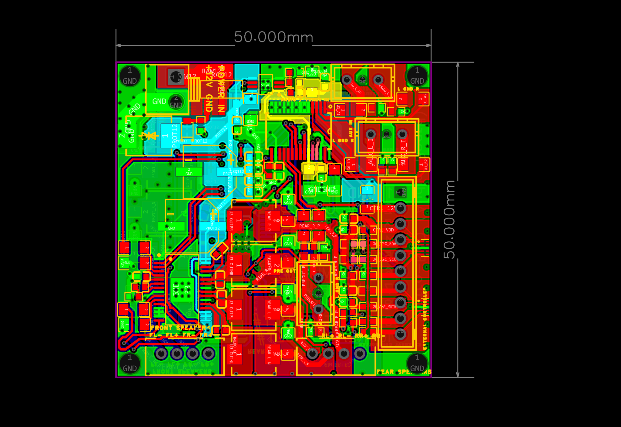
PCB design
RP2040 routing and assembly design views document electrical interfaces and component placement.
Project detailsTalk engineering
Send a short, non-confidential summary of your requirements and current development stage.
Discuss your project with AUBRIX